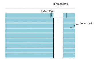
Plated through-holes (PTH) connect together the top, bottom, and any required internal conductor layers. PTHs are drilled oversize to accommodate the thickness of the copper plating that will cover the entire barrel of the hole as well as the surface of the outer pads. Exterior pads maybe plated along with the entire foil surface or selectively plated just at the PTH side.

Plated through-holes (PTH) connect together the top, bottom, and any required internal conductor layers. PTHs are drilled oversize to accommodate the thickness of the copper plating that will cover the entire barrel of the hole as well as the surface of the outer pads. Exterior pads maybe plated along with the entire foil surface or selectively plated just at the PTH side.
Section: The main purpose of a PTH is to interconnect or connect to other circuits.
Section: A PTH must have adequate copper coverage on the inside with a smooth trace that connects to the top and bottom circuit layer.
Section: PTH’s in multi-layer PCB structures are mostly used on the outer layers.
Section: A PTH or via can have either one, two or three parallel traces.
Section: The inner layers are interconnected through vias that transmit signals between layers. These are also called blind vias if they do not extend to the outer layer.
Section: A via must be round in shape and conform to the minimum annular ring requirement. This means that there should be a defined annular ring around the drilled hole with dimensions greater than those specified based on the specified drill diameter and thickness of the copper layer being drilled.
Section: VIPPO is a term used to describe how stacked vias would cause a signal path misalignment due to different width traces on each layer of the stackup.
Section: The recommended clearance between two vias is 0.20mm (0.008 inch) when they are placed adjacent to each other, measured from edge-to


 2022-11-08
 BEST
BEST

.png)
.png)
.png)
.png)

.png)

