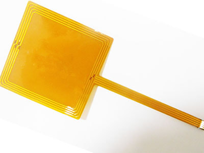
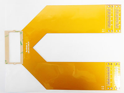
When designing a flex PCB stackup, you may face some restrictions in enhancing the reliability of the board. Today, we will discuss the ways to improve the reliability of a board by increasing the flexibility and improving design considerations of a multilayer PCB stackup. These steps can be implemented for PCB stackup designs as seen in 8 layer flex PCBs.
flexible circuits
Improve Flexibility by Reducing Overall Thickness
All or some of the below mentioned steps can be executed to lower the overall thickness of the PCB. A thinner PCB stackup will allow it to be more flexible.
1.Reduce the base copper weight.
2.Reduce the adhesive thickness.
3.Reduce the dielectric material thickness.
4.Using adhesiveless base materials can reduce the thickness of the substrate by 1-2 mils, which is almost 25-50μm.
5.Make use of selective plating to avoid copper plating the conductors.
Improve Reliability by Reinforcing the PCB
Here, the boards, components, and the layout should be designed to deliver a robust structure that can withstand flexing.
1.The weight on both sides of the PCB should be equal. This includes the weight of the conductors and the material.
2.The conductors on different layers of a PCB should not be placed on top of each other. Instead, they should be placed in a staggered pattern.
3.Conductor thickness should always be constant in and near the bend areas.
4.There should be no plated-through holes in the bend areas.
5.There should be no discontinuities near the bend.
6.Traditional copper can be proved to reduce the flexibility of a PCB. Opt for screened-on coatings like silver epoxy.
7.For slits in the circuit, reliefs or tear stops need to be built into the PCB.
flexible pcb
Tight tolerances will have to be put in place to ensure that your stacked up PCB can provide flexibility as well as reliability. Several of the above-mentioned steps can easily be incorporated in the designing process itself. Your PCB manufacturer should be able to help you with the most appropriate improvements for your application.


 2023-03-22
 BEST
BEST


.png)
.png)
.png)
.png)

.png)

